To continue our quest, we want to implement some of the most used (or at least used for the most popular games) mappers of the NES. For now, we will choose MMC1 and MMC3, a rather simple, and a rather complex mapper.
mmc1
The MMC1 mapper is a mapper, that offers banking for PRG and CHR ROM. This means, the actual memory behind the (mapped) addresses can be changed from the mapper, thus giving us possibly a lot more space on the cartridge.
CPU $6000-$7FFF: 8 KB PRG RAM bank, (optional)
CPU $8000-$BFFF: 16 KB PRG ROM bank, either switchable or fixed to the first bank
CPU $C000-$FFFF: 16 KB PRG ROM bank, either fixed to the last bank or switchable
PPU $0000-$0FFF: 4 KB switchable CHR bank
PPU $1000-$1FFF: 4 KB switchable CHR bank
We get the amount of banks of the PRG banks (16kb) and of the CHR banks (8kb) from the iNES header, more precisely byte 4 and 5 of the header.
MMC1 has a quirk, where it will take 5 writes to collect all the bits for the actual write that sets a bank. These 5 writes all are made to the Load register (0x8000-0xffff) that consists of a shift register. Each write to the load register shifts the rightmost bit onto said shift register, and on the 5th write, the whole shift register is evaluated.
if (adr >= 0x8000 && adr <= 0xffff) {
		//	resetting shift register
		if (val & 0b10000000) {
			shift_register = 0b10000;
			sr_write_counter = 0;
			return;
		}
		//	shifting 4 times, writing on the 5th
		else {
			sr_write_counter++;
			shift_register = ((shift_register >> 1) | ((val & 1) << 4)) & 0b11111;
...
There are 4 address areas which control the following settings:
Control (0x8000-0x9fff)
4bit0
-----
CPPMM
|||||
|||++- Mirroring (0: one-screen, lower bank; 1: one-screen, upper bank;
|||               2: vertical; 3: horizontal)
|++--- PRG ROM bank mode (0, 1: switch 32 KB at $8000, ignoring low bit of bank number;
|                         2: fix first bank at $8000 and switch 16 KB bank at $C000;
|                         3: fix last bank at $C000 and switch 16 KB bank at $8000)
+----- CHR ROM bank mode (0: switch 8 KB at a time; 1: switch two separate 4 KB banks)
CHR bank 0 (0xa000-0xbfff)
4bit0
-----
CCCCC
|||||
+++++- Select 4 KB or 8 KB CHR bank at PPU $0000 (low bit ignored in 8 KB mode)
CHR bank 1 (0xc000-0xdfff)
4bit0
-----
CCCCC
|||||
+++++- Select 4 KB CHR bank at PPU $1000 (ignored in 8 KB mode)
PRG bank (0xe000-0xffff)
4bit0
-----
RPPPP
|||||
|++++- Select 16 KB PRG ROM bank (low bit ignored in 32 KB mode)
+----- PRG RAM chip enable (0: enabled; 1: disabled; ignored on MMC1A)
So, we are able to decide, which memory addresses have a fixed bank, and which are switchable. And the banks that are switchable, we can select through the bank selector. So, when we read from memory, we can tell our mapper to select the appropriate PRG and CHR banks on-the-fly.
virtual unsigned char read(uint16_t adr) {
	if (PRGsize == 0x4000) {
		//	First PRG area
		if (adr >= 0x8000 && adr <= 0xbfff) {
			//	this area is fixed to the first PRG bank
			if (PRGswitchAddr == 0xc000) {
				return m[(adr % 0x8000) + 0x10];
			}
			//	this area is switchable
			else {
				return m[(adr % 0x8000) + PRGid * PRGsize + 0x10];
			}
		}
		//	Second PRG area
		else if (adr >= 0xc000 & adr <= 0xffff) {
			//	this area is fixed to the last PRG bank
			if (PRGswitchAddr == 0x8000) {
				return m[(adr % 0xc000) + 0x10 + (romPRG16ks - 1) * PRGsize];
			}
			//	this area is switchable
			else {
				return m[(adr % 0x8000) + PRGid * PRGsize + 0x10];
			}
		}
		else {
			return memory[adr];
		}
	}
	//	32k PRG banks
	else if (PRGsize == 0x8000) {
		if (adr >= 0x8000 && adr <= 0xffff) {
			return m[(adr % 0x8000) + 0x10 + PRGid * PRGsize];
		}
		else {
			return memory[adr];
		}
	}
}
Note:
The '0x10' in the reads, is the skipped iNES header.
The 'romPRG16ks' is the amount of banks we get from the iNES header.
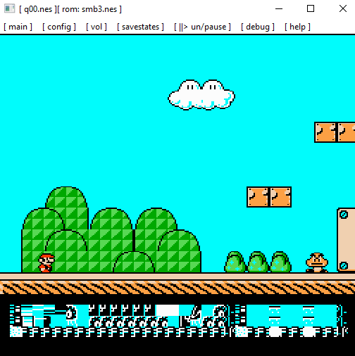
This is the whole concept of the MMC1 mapper. After we successfully implemented this mapper, we are able to boot “Zelda“.
mmc3
This mapper allows even more PRG and CHR banks to be selected, but doesn’t have the 5-write-quirk of MMC1. It does, though, have a scanline counter, which can trigger an IRQ on decrementing.
First of all, the addressable banks:
CPU $6000-$7FFF: 8 KB PRG RAM bank (optional)
CPU $8000-$9FFF (or $C000-$DFFF): 8 KB switchable PRG ROM bank
CPU $A000-$BFFF: 8 KB switchable PRG ROM bank
CPU $C000-$DFFF (or $8000-$9FFF): 8 KB PRG ROM bank, fixed to the second-last bank
CPU $E000-$FFFF: 8 KB PRG ROM bank, fixed to the last bank
PPU $0000-$07FF (or $1000-$17FF): 2 KB switchable CHR bank
PPU $0800-$0FFF (or $1800-$1FFF): 2 KB switchable CHR bank
PPU $1000-$13FF (or $0000-$03FF): 1 KB switchable CHR bank
PPU $1400-$17FF (or $0400-$07FF): 1 KB switchable CHR bank
PPU $1800-$1BFF (or $0800-$0BFF): 1 KB switchable CHR bank
PPU $1C00-$1FFF (or $0C00-$0FFF): 1 KB switchable CHR bank
To select the banks, we can write to the Bank Register (0x8000-0x9fff). The writes are differentiated in even and odd, e.g. even 0x8000, 0x8202, etc, odd 0x8001, 0x8333 etc.
Even writes
7  bit  0
---- ----
CPMx xRRR
|||   |||
|||   +++- Specify which bank register to update on next write to Bank Data register
|||        0: Select 2 KB CHR bank at PPU $0000-$07FF (or $1000-$17FF);
|||        1: Select 2 KB CHR bank at PPU $0800-$0FFF (or $1800-$1FFF);
|||        2: Select 1 KB CHR bank at PPU $1000-$13FF (or $0000-$03FF);
|||        3: Select 1 KB CHR bank at PPU $1400-$17FF (or $0400-$07FF);
|||        4: Select 1 KB CHR bank at PPU $1800-$1BFF (or $0800-$0BFF);
|||        5: Select 1 KB CHR bank at PPU $1C00-$1FFF (or $0C00-$0FFF);
|||        6: Select 8 KB PRG ROM bank at $8000-$9FFF (or $C000-$DFFF);
|||        7: Select 8 KB PRG ROM bank at $A000-$BFFF
||+------- Nothing on the MMC3, see MMC6
|+-------- PRG ROM bank mode (0: $8000-$9FFF swappable,
|                                $C000-$DFFF fixed to second-last bank;
|                             1: $C000-$DFFF swappable,
|                                $8000-$9FFF fixed to second-last bank)
+--------- CHR A12 inversion (0: two 2 KB banks at $0000-$0FFF,                                  four 1 KB banks at $1000-$1FFF;
                              1: two 2 KB banks at $1000-$1FFF,                                  four 1 KB banks at $0000-$0FFF)
So, with even writes we will dictate which bank will be changed, which PRG mode will be used, and if CHR A12 inversion is used or not.
The selection of these banks isn’t straightforward though, it’s depending on PRG mode and CHR A12 inversion, as can be seen in the following table.
| CHR A12 inversion | unused | used |
|---|---|---|
| PPU Bank | Value of MMC3 register | |
| $0000-$03FF | R0 | R2 |
| $0400-$07FF | R3 | |
| $0800-$0BFF | R1 | R4 |
| $0C00-$0FFF | R5 | |
| $1000-$13FF | R2 | R0 |
| $1400-$17FF | R3 | |
| $1800-$1BFF | R4 | R1 |
| $1C00-$1FFF | R5 | |
| PRG bank mode | 0 | 1 |
|---|---|---|
| CPU Bank | Value of MMC3 register | |
| $8000-$9FFF | R6 | (-2) |
| $A000-$BFFF | R7 | R7 |
| $C000-$DFFF | (-2) | R6 |
| $E000-$FFFF | (-1) | (-1) |
(-1) : the last bank
(-2) : the second last bank
Odd writes
These writes, simply enough, are the bank number to the bank position that was select with the even write before.
irq / scanline counter
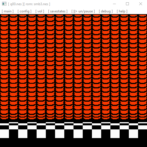
The scanline counter is used, for example, by Super Mario Bros. 3, to identify the position of the UI at the bottom. The UI will look garbled, if this function is not implemented, as we will see later on.
IRQ latch (0xc000-0xdfff, even)
This register holds the value, that will be loaded into the actual scanline counter when a reload is forced, or when the counter reached zero.
IRQ reload (0xc000-0xdfff, odd)
This register resets the actual scanline counter, and will push the IRQ latch value to the counter in the next scanline.
IRQ disable (0xe000-0xffff, even)
Writing to this register will disable the IRQ generation and also remove any pending IRQs.
IRQ enable (0xe000-$ffff, odd)
Writing to this address area will enable IRQ generation again.
In code, this will look something like this:
else if (adr >= 0xc000 && adr <= 0xdfff) {
	//	set reload value | even
	if ((adr % 2) == 0) {
		irq_latch = val;
	}
	//	actually set reload value to scanline counter | odd
	else {
		irq_reload_pending = true;
		irq_counter = 0;
	}
}
else if (adr >= 0xe000 && adr <= 0xffff) {
	//	IRQ disable | even
	if ((adr % 2) == 0) {
		irq_enabled = false;
		irq_assert = false;
	}
	//	IRQ enable | odd
	else {
		irq_enabled = true;
	}
}
scanline counter
The actual ticking of the scanline counter happens on every visible scanline, plus the prep-scanline, on cycle 260 of each line. The actual evaluation of the scanline counter is shown in code here, as this can often leads to problems and bugs, which may be hard to debug, due to conflicting documentation.
Note that, the nextScanline() function is only called, when either BG or Sprites are to be drawn (dictated from PPUMASK).
if (ppuScanline >= 0 && ppuScanline <= 239) {
	if (ppuCycles == 230) {
		renderScanline(ppuScanline);
	}
	else if (ppuCycles == 260 && (PPU_MASK.show_bg || PPU_MASK.show_sprites)) {
		nextScanline();
	}
}
virtual void nextScanline() {
	if (irq_counter == 0 || irq_reload_pending) {
		irq_counter = irq_latch;
		irq_reload_pending = false;
	}
	else {
		irq_counter--;
	}

	if (irq_counter == 0 && irq_enabled) {
		irq_assert = true;
	}
}
virtual bool IRQ() {
	bool isIRQ = irq_assert;
	irq_assert = false;

	return isIRQ;
}
This way, we are able to check for pending IRQs in our CPU. If the CPU detects a pending IRQ, it will (almost) do the same procedure as on an NMI. It will push the PC to the stack, push P / PSW to the stack, and jump to the Interrupt Vector, that is located at 0xfffe / 0xffff, and finally enable the interruptDisable flag of the PPUSTATUS.
If the IRQ and the scanline counter are implemented correctly, we will be able to boot Super Mario Bros. 3.
mapper 37 (mmc3 subtype)
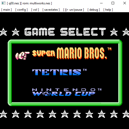
So, there exists a subtype (there are actually multiple subtypes of MMC3) of the MMC3 mapper, I have a personal interest in, because it was my first cartridge for my NES, that european readers might recognize. It’s the multi-game cartridge, filled with Super Mario Bros., Tetris, and World Cup.

This mapper, is a complete MMC3 mapper, but it has an additional function, which is to select the outer bank. This makes it easy, to restrict the games to their own “memory cells”.
Outer Bank Select (0x6000-0x7fff)
7  bit  0
xxxx xQBB
      │││
      │└┴── If 3, forces PRG A16 high regardless of Q bit; otherwise
      └──── the MMC3's PRG A16 is ANDed with this bit before going to PRG ROM.
             Additionally connected to A17 on both PRG and CHR ROM.
This results in memory being addressable like this:
| Value written | PRG window | 128kB CHR window |
|---|---|---|
| 0,1,2 | $00000-$0FFFF (64kB) | $00000-$1FFFF |
| 3 | $10000-$1FFFF (64kB) | $00000-$1FFFF |
| 4,5,6 | $20000-$3FFFF (128kB) | $20000-$3FFFF |
| 7 | $30000-$3FFFF (64kB) | $20000-$3FFFF |
So, if we add this little feature, we will also be able, to boot the multi-game cartridge, which, indeed, is the only cartridge to ever use this mapper! 😉
Comments