Of course our first action needs to be implementing all of the opcodes the 6502 offers. The first thing I noticed was the different addressing modes the 6502 has.
| immediate | This is the address right after the opcode (PC+1) |
| zeropage | This is the address of the value at PC+1. (8 bit force it to be on zeropage, 0x00nn) |
| zeropage, x-indexed | Same as zeropage, but offset with register X |
| zeropage, y-indexed | Same as zeropage, but offset with register Y |
| indirect, x-indexed | Read the value of the immediate byte. Use this value + X (low nibble), and this value + X + 1 (high nibble) as an address |
| indirect, y-indexed | Read the value of the immediate byte. Use this value (low nibble), and this value + 1 (high nibble) as an address. Add Y to this address |
| absolute | This gives a complete address with the next 2 bytes (little Endian, so low nibble comes first) |
| absolute, x-indexed | Same as absolute, but offset with register X |
| absolute, y-indexed | Same as absolute, but offset with register Y |
For comfort, I just implemented each addressing mode as a function in the MMU, so whenever we need to address something, no matter if it is for a read or a write, we can just get the desired address by passing the values to our addressing functions.
unsigned char readFromMem(uint16_t adr);
uint16_t getImmediate(uint16_t adr);
uint16_t getZeropage(uint16_t adr);
uint16_t getZeropageXIndex(uint16_t adr, uint8_t X);
uint16_t getZeropageYIndex(uint16_t adr, uint8_t Y);
uint16_t getIndirectXIndex(uint16_t adr, uint8_t X);
uint16_t getIndirectYIndex(uint16_t adr, uint8_t Y);
uint16_t getAbsolute(uint16_t adr);
uint16_t getAbsoluteXIndex(uint16_t adr, uint8_t X);
uint16_t getAbsoluteYIndex(uint16_t adr, uint8_t Y);
With this done, we can now start implementing the opcodes of the 6502, which turn out to be quite a few less than on the Gameboy.
| x0 | x1 | x2 | x3 | x4 | x5 | x6 | x7 | x8 | x9 | xA | xB | xC | xD | xE | xF | |
| 0x | 1 BRKimp 7 NV1BDIZC BI |
2 ORAinx 6 NV1BDIZC NZ |
KIL | SLO inx |
NOP zp |
2 ORAzp 3 NV1BDIZC NZ |
2 ASLzp 5 NV1BDIZC CNZ |
SLO zp |
1 PHPimp 3 NV1BDIZC |
2 ORAimm 2 NV1BDIZC NZ |
1 ASLakk 2 NV1BDIZC CNZ |
ANC imm |
NOP abs |
3 ORAabs 4 NV1BDIZC NZ |
3 ASLabs 6 NV1BDIZC CNZ |
SLO abs |
| 1x | 3 BPLrel 2*+ NV1BDIZC |
2 ORAiny 5+ NV1BDIZC NZ |
KIL | SLO iny |
NOP zpx |
2 ORAzpx 4 NV1BDIZC NZ |
2 ASLzpx 6 NV1BDIZC CNZ |
SLO zpx |
1 CLCimp 2 NV1BDIZC C |
3 ORAaby 4+ NV1BDIZC NZ |
NOP imp |
SLO aby |
NOP abx |
3 ORAabx 4+ NV1BDIZC NZ |
3 ASLabx 7 NV1BDIZC CNZ |
SLO abx |
| 2x | 3 JSRabs 6 NV1BDIZC |
2 ANDinx 6 NV1BDIZC NZ |
KIL | RLA inx |
2 BITzp 3 NV1BDIZC NOZ |
2 ANDzp 3 NV1BDIZC NZ |
2 ROLzp 5 NV1BDIZC CNZ |
RLA zp |
1 PLPimp 4 NV1BDIZC CNVZIBD |
2 ANDimm 2 NV1BDIZC NZ |
1 ROLakk 2 NV1BDIZC CNZ |
ANC imm |
3 BITabs 4 NV1BDIZC NVZ |
3 ANDabs 4 NV1BDIZC NZ |
3 ROLabs 6 NV1BDIZC CNZ |
RLA abs |
| 3x | 3 BMIrel 2*+ NV1BDIZC |
2 ANDiny 5+ NV1BDIZC NZ |
KIL | RLA iny |
NOP zpx |
2 ANDzpx 4 NV1BDIZC NZ |
2 ROLzpx 6 NV1BDIZC CNZ |
RLA zpx |
1 SECimp 2 NV1BDIZC C |
3 ANDaby 4+ NV1BDIZC NZ |
NOP imp |
RLA aby |
NOP abx |
3 ANDabx 4+ NV1BDIZC NZ |
3 ROLabx 7 NV1BDIZC CNZ |
RLA abx |
| 4x | 1 RTIimp 6 NV1BDIZC CNVZIBD |
2 EORinx 6 NV1BDIZC NZ |
KIL | SRE inx |
NOP zp |
1 EORzp 3 NV1BDIZC NZ |
2 LSRzp 5 NV1BDIZC CNZ |
SRE zp |
1 PHAimp 3 NV1BDIZC |
2 EORimm 2 NV1BDIZC NZ |
1 LSRakk 2 NV1BDIZC CNZ |
ALR imm |
3 JMPabs 3 NV1BDIZC |
3 EORabs 4 NV1BDIZC NZ |
3 LSRabs 6 NV1BDIZC CNZ |
SRE abs |
| 5x | 3 BVCrel 2*+ NV1BDIZC |
2 EORiny 5+ NV1BDIZC NZ |
KIL | SRE iny |
NOP zpx |
2 EORzpx 4 NV1BDIZC NZ |
2 LSRzpx 6 NV1BDIZC CNZ |
SRE zpx |
1 CLIimp 2 NV1BDIZC I |
3 EORaby 4+ NV1BDIZC NZ |
NOP imp |
SRE aby |
NOP abx |
3 EORabx 4+ NV1BDIZC NZ |
3 LSRabx 7 NV1BDIZC CNZ |
SRE abx |
| 6x | 1 RTSimp 6 NV1BDIZC |
2 ADCinx 6 NV1BDIZC CNVZ |
KIL | RRA inx |
NOP zp |
1 ADCzp 3 NV1BDIZC CNVZ |
2 RORzp 5 NV1BDIZC CNZ |
RRA zp |
1 PLAimp 4 NV1BDIZC NZ |
2 ADCimm 2 NV1BDIZC CNVZ |
1 RORakk 2 NV1BDIZC CNZ |
ARR imm |
3 JMPind 5 NV1BDIZC |
3 ADCabs 4 NV1BDIZC CNVZ |
3 RORabs 6 NV1BDIZC CNZ |
RRA abs |
| 7x | 3 BVSrel 2*+ NV1BDIZC |
2 ADCiny 5+ NV1BDIZC CNVZ |
KIL | RRA iny |
NOP zpx |
2 ADCzpx 4 NV1BDIZC CNVZ |
2 RORzpx 6 NV1BDIZC CNZ |
RRA zpx |
1 SEIimp 2 NV1BDIZC I |
3 ADCaby 4+ NV1BDIZC CNVZ |
NOP imp |
RRA aby |
NOP abx |
3 ADCabx 4+ NV1BDIZC CNVZ |
3 RORabx 7 NV1BDIZC CNZ |
RRA abx |
| 8x | NOP imm |
2 STAinx 6 NV1BDIZC |
NOP imm |
SAX inx |
2 STYzp 3 NV1BDIZC |
2 STAzp 3 NV1BDIZC |
2 STXzp 3 NV1BDIZC |
SAX zp |
1 DEYimp 2 NV1BDIZC NZ |
NOP imm |
1 TXAimp 2 NV1BDIZC NZ |
XAA imm |
3 STYabs 4 NV1BDIZC |
3 STAabs 4 NV1BDIZC |
3 STXabs 4 NV1BDIZC |
SAX abs |
| 9x | 3 BCCrel 2*+ NV1BDIZC |
2 STAiny 6 NV1BDIZC |
KIL | AHX iny |
2 STYzpx 4 NV1BDIZC |
2 STAzpx 4 NV1BDIZC |
2 STXzpy 4 NV1BDIZC |
SAX zpy |
1 TYAimp 2 NV1BDIZC NZ |
3 STAaby 5 NV1BDIZC |
1 TXSimp 2 NV1BDIZC |
TAS aby |
SHY abx |
3 STAabx 5 NV1BDIZC |
SHX aby |
AHX aby |
| Ax | 2 LDYimm 2 NV1BDIZC NZ |
2 LDAinx 6 NV1BDIZC NZ |
2 LDXimm 2 NV1BDIZC NZ |
LAX inx |
2 LDYzp 3 NV1BDIZC NZ |
2 LDAzp 3 NV1BDIZC NZ |
1 LDXzp 3 NV1BDIZC NZ |
LAX zp |
1 TAYimp 2 NV1BDIZC NZ |
2 LDAimm 2 NV1BDIZC NZ |
1 TAXimp 2 NV1BDIZC NZ |
LAX imm |
3 LDYabs 4 NV1BDIZC NZ |
3 LDAabs 4 NV1BDIZC NZ |
3 LDXabs 4 NV1BDIZC NZ |
LAX abs |
| Bx | 3 BCSrel 2*+ NV1BDIZC |
2 LDAiny 5+ NV1BDIZC NZ |
KIL | LAX iny |
2 LDYzpx 4 NV1BDIZC CZ |
2 LDAzpx 4 NV1BDIZC NZ |
2 LDXzpy 4 NV1BDIZC NZ |
LAX zpy |
1 CLVimp 2 NV1BDIZC V |
3 LDAaby 4+ NV1BDIZC NZ |
1 TSXimp 2 NV1BDIZC NZ |
LAS aby |
3 LDYabx 4+ NV1BDIZC NZ |
3 LDAabx 4+ NV1BDIZC NZ |
3 LDXaby 4+ NV1BDIZC NZ |
LAX aby |
| Cx | 2 CPYimm 2 NV1BDIZC CNZ |
2 CMPinx 6 NV1BDIZC CNZ |
NOP imm |
DCP inx |
2 CPYzp 3 NV1BDIZC CNZ |
1 CMPzp 3 NV1BDIZC CNZ |
2 DECzp 5 NV1BDIZC NZ |
DCP zp |
1 INYimp 2 NV1BDIZC NZ |
2 CMPimm 2 NV1BDIZC CNZ |
1 DEXimp 2 NV1BDIZC NZ |
AXS imm |
3 CPYabs 4 NV1BDIZC CNZ |
3 CMPabs 4 NV1BDIZC CNZ |
3 DECabs 6 NV1BDIZC NZ |
DCP abs |
| Dx | 3 BNErel 2*+ NV1BDIZC |
2 CMPiny 5+ NV1BDIZC CNZ |
KIL | DCP iny |
NOP zpx |
2 CMPzpx 4 NV1BDIZC CNZ |
2 DECzpx 6 NV1BDIZC NZ |
DCP zpx |
1 CLDimp 2 NV1BDIZC D |
3 CMPaby 4+ NV1BDIZC CNZ |
NOP imp |
DCP aby |
NOP abx |
3 CMPabx 4+ NV1BDIZC CNZ |
3 DECabx 7 NV1BDIZC NZ |
DCP abx |
| Ex | 2 CPXimm 2 NV1BDIZC CNZ |
2 SBCinx 6 NV1BDIZC CNVZ |
NOP imm |
ISC inx |
2 CPXzp 3 NV1BDIZC CNZ |
2 SBCzp 3 NV1BDIZC CNVZ |
2 INCzp 5 NV1BDIZC NZ |
ISC zp |
1 INXimp 2 NV1BDIZC NZ |
2 SBCimm 2 NV1BDIZC CNVZ |
1 NOPimp 2 NV1BDIZC |
SBC imm |
3 CPXabs 4 NV1BDIZC CNZ |
3 SBCabs 4 NV1BDIZC CNVZ |
3 INCabs 6 NV1BDIZC NZ |
ISC abs |
| Fx | 3 BEQrel 2*+ NV1BDIZC |
2 SBCiny 5+ NV1BDIZC CNVZ |
KIL | ISC iny |
NOP zpx |
2 SBCzpx 4 NV1BDIZC CNVZ |
2 INCzpx 6 NV1BDIZC NZ |
ISC zpx |
1 SEDimp 2 NV1BDIZC D |
3 SBCaby 4+ NV1BDIZC CNVZ |
NOP imp |
ISC aby |
NOP abx |
3 SBCabx 4+ NV1BDIZC CNVZ |
3 INCabx 7 NV1BDIZC NZ |
ISC abx |
The legal opcodes are linked to the description. The illegal opcodes are grey and not important for the moment. The address mode is in the bottom left, the timing in the bottom right. “+” indicates another cycle on a page boundary breach, “*” indicates another cycle, if the branch is taken. The affected flags are colored red at the bottom.
| BRK | Sets a software interrupt with Break-Flag |
| ORA | Bitwise OR to the accumulator |
| ASL | Shifts the value to the left, into Carry-Flag |
| PHP | Puts the Status-Register (Flags) onto the stack |
| BPL | Branches if negative flag is cleared |
| ASL | Rotates the value to the left, into Carry-Flag |
| CLC | Clears the Carry-Flag |
| ASL | Jumps to Sub-Routine |
| AND | Bitwise AND to the accumulator |
| BIT | Bit 7 of value to N-Flag, Bit 6 to V-Flag, and bitwise AND accumulator and value to Z-Flag |
| ROL | Rotates the value to the left, into Carry-Flag, old Carr-Flag value to bit 0 |
| PLP | Loads into Status-Register (Flags) from the stack |
| BMI | Branches if negative flag is set |
| SEC | Sets the Carry-Flag |
| RTI | Returns from Interrupt |
| EOR | Bitwise XOR to the accumulator |
| LSR | Shifts the value to the right, into Carry-Flag |
int stepCPU() {
	switch (readFromMem(PC)) {
		case 0x29: { PC++; return AND(getImmediate(PC), 2); PC++; break; }
		case 0x2d: { PC++; return AND(getAbsolute(PC), 2); PC += 4; break; }
		case 0x39: { PC++; return AND(getAbsoluteYIndex(PC, registers.Y), 4); PC += 2; break; }		//	TODO +1 cyc if page boundary is crossed
		case 0x3d: { PC++; return AND(getAbsoluteXIndex(PC, registers.X), 4); PC += 2; break; }		//	TODO +1 cyc if page boundary is crossed
...
Most of the opcodes are fairly easy to implement, probably only ADC and SBC are the ones, that might give a headache.
ADC adds the value of the memory at the given address to the accumulator, plus the carry bit as well. Where SBC does the same, only subtracting the values from the accumulator. Therefore we can just write the ADC function, and use an inverted value as argument for it, to use it as SBC as well.
uint8_t ADD(uint8_t val, uint8_t cycles) {
	//	TODO handle bcd when decimal flag is set
	uint16_t sum = registers.A + val + status.carry;
	status.setOverflow((~(registers.A ^ val) & (registers.A ^ sum) & 0x80) > 0);
	status.setCarry(sum > 0xff);
	registers.A = sum;
	status.setZero(registers.A == 0);
	status.setNegative(registers.A >> 7);
	return cycles;
}
uint8_t ADC(uint16_t adr, uint8_t cycles) {
	return ADD(readFromMem(adr), cycles);
}
uint8_t SBC(uint16_t adr, uint8_t cycles) {
	return ADD(~readFromMem(adr), cycles);
}
The flags affected are zero, negative, carry and overflow (also decimal is important, but will be later added, when we use this CPU for the C64 emulation, as the NES’s CPU wasn’t capable of using this, probably just by a cut trace on the PCB).
| zero | is set when the result is zero |
| negative | is always bit 7 (0-based) of the result |
| carry | is set when we have a carry, meaning that we can’t represent the result with 8 bits, therefore we check if the result is greater than 0xFF |
| overflow | is set, when if two inputs with the same sign, produce a result with a different sign. So the flag actually represents that the sign of the outcome is wrong |
Note: You can never have an overflow flag set, when the two inputs have different signs, as the range does not allow it.
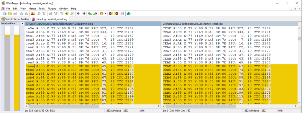
For testing purposes I ran nestest, a testing ROM for almost all CPU behaviors. (Credits go to Kevin Horton, sadly I was unable to find a github or something else to link him to. Make sure to read his README)
Nestest provides a log file, with a proper output, that way, we can compare our output to it, and see how well it matches, and where our CPU might be going wrong.
Comments