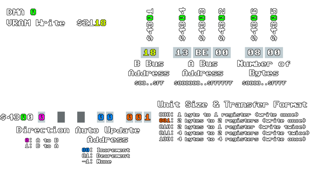
As most systems the SNES also offers to run DMAs, so Direct Memory Access, which are a fast way of copying stuff from one place to another, without a necessary man-in-the-middle. Since we want to run and test our PPU and its function with krom’s tests, we will need to make our DMAs work.
There are also H-DMAs, so DMAs that happen only during horizontal blanking. Those won't be covered here, but in a later chapter, when they will be used to create more advanced image effects.
The system offers 8 individual, bi-directional DMAs. They can be started by writing the appropriate bit to register 0x420B, so bit 6 starts DMA6, bit 2 starts DMA2 and so on.
The registers 0x43x0 are used to configure each DMA individually, where x is the ID of the DMA, so DMA5 is configured on 0x4350 and so on.
The actual bits on these registers are used to set the following settings:
| 7 | Transfer Direction (0=A:CPU to B:I/O, 1=B:I/O to A:CPU) |
| 6 | Addressing Mode (0=Direct Table, 1=Indirect Table) (HDMA only) |
| 5 | Unused |
| 4-3 | A-BUS Address Step (0=Increment, 2=Decrement, 1/3=None) (DMA only) |
| 2-0 | Unit Size & Transfer Format |
The Unit Size & Transfer Format defines the size and the pattern of what the DMA will transfer in every step, and has the follwing settings:
| 000 | Transfer 1 Byte | xx | e.g. WRAM |
| 001 | Transfer 2 Bytes | xx, xx+1 | e.g VRAM |
| 010 | Transfer 2 Bytes | xx, xx | e.g. OAM or CGRAM |
| 011 | Transfer 4 Bytes | xx, xx, xx+1, xx+1 | e.g. BGnxOFS |
| 100 | Transfer 4 Bytes | xx, xx+1, xx+2, xx+3 | e.g. BGnSC |
| 101 | Transfer 4 Bytes | xx, xx+1, xx, xx+1 | Reserved |
| 110 | Transfer 2 Bytes | xx, xx | Reserved, same as Mode 2 |
| 111 | Transfer 4 Bytes | xx, xx, xx+1, xx+1 | Reserved, same as Mode 3 |
The additional registers to set up the DMA are the following:
| 0x43x1 | Address of the B-Bus (e.g. VRAM Write is 0x2118, so 0x18) |
| 0x43x2 | Lower Byte of A-Bus Address (CPU address space) |
| 0x43x3 | Upper Byte of A-Bus Address (CPU address space) |
| 0x43x4 | Bank Byte of A-Bus Address (CPU address space) |
| 0x43x5 | Lower Byte of Number of Bytes to Transfer |
| 0x43x6 | Upper Byte of Number of Bytes to Transfer |
So for example, if we wanted to transfer 0x800 bytes from 0x13BE00 to VRAM, the completely set up DMA would look like this (and would only need to be started by writing bit 0 of 0x420B)

The final function that is triggered by the writes to 0x420B could then look something like this:
void startDMA() {
	for (u8 i = 0; i < 8; i++) {
		if ((memory[0x420b] & (1 << i)) == (1 << i)) {
			u8 _IO = memory[0x4301 + (i * 0x10)];
			u8 _v = memory[0x4300 + (i * 0x10)];
			u8 dma_dir = _v >> 7;				//	0 - write to IO, 1 - read from IO
			u8 dma_step = (_v >> 3) & 0b11;		//	0 - increment, 2 - decrement, 1/3 = none
			u8 dma_mode = (_v & 0b111);
			u32 target_adr = (memory[0x4304 + (i * 0x10)] << 16) | (memory[0x4303 + (i * 0x10)] << 8) | memory[0x4302 + (i * 0x10)];
			//	count bytes
			u16 c = (memory[0x4306 + (i * 0x10)] << 8) | memory[0x4305 + (i * 0x10)];
			switch (dma_mode) {
			case 0: {				//	transfer 1 byte (e.g. WRAM)
				while (((memory[0x4306 + (i * 0x10)] << 8) | memory[0x4305 + (i * 0x10)]) > 0) {		//	read bytes count
					if (!dma_dir)
						writeToMem(memory[target_adr], 0x2100 + _IO);
					else
						writeToMem(readFromMem(0x2100 + _IO), target_adr);
					c--;
					memory[0x4306 + (i * 0x10)] = c >> 8;
					memory[0x4305 + (i * 0x10)] = c & 0xff;
					target_adr += (dma_step == 0) ? 1 : ((dma_step == 2) ? -1 : 0);
				}
				break;
			}
			case 1:					//	transfer 2 bytes (xx, xx + 1) (e.g. VRAM)
				while (((memory[0x4306 + (i * 0x10)] << 8) | memory[0x4305 + (i * 0x10)]) > 0) {		//	read bytes count
					if (!dma_dir) {
						writeToMem(memory[target_adr], 0x2100 + _IO);
						if (!--c) return;
						writeToMem(memory[target_adr + 1], 0x2100 + _IO + 1);
						if (!--c) return;
					}
					else {
						writeToMem(readFromMem(0x2100 + _IO), target_adr);
						if (!--c) return;
						writeToMem(readFromMem(0x2100 + _IO + 1), target_adr + 1);
						if (!--c) return;
					}
					memory[0x4306 + (i * 0x10)] = c >> 8;
					memory[0x4305 + (i * 0x10)] = c & 0xff;
					target_adr += (dma_step == 0) ? 2 : ((dma_step == 2) ? -2 : 0);
				}
				break;

...

Comments