cartridge loading
So, we got our CPU running, confirmed by nestest. Time to load a real ROM game dump.
For starters, we will work with NROM games, the simplest mapper there is, before we will actually implement other mappers, that might be more complex (multiples ROM/RAM banks, multiple banks for VRAM etc.)
I will use “Donkey Kong” for testing, because it doesn’t use scrolling, or other advanced features. So, to load the cartridge, we can use about the same loading technique as for nestest.
//	copy cartridge to memory
void loadROM(unsigned char c[]) {
	for (int i = 0; i < 0x4000; i++) {
		//	NROM
		memory[0xc000 + i] = c[i+0x10];
	}
	for (int i = 0; i < 0x2000; i++) {
		//	NROM
		writeCHRRAM(c, 0x4010);
	}
}
As you can see, we copy the first 16k of the ROM to 0xc000. It’s important (for now) to additionally add an offset of 0x10, because we have 16 bytes of ines header at the very beginning of the ROM, which we will handle properly later on.
pattern tables
We also copy the first 8k of the ROM to the Pattern Table (CHR ROM), which is necessary for this mapper (NROM).
The CHR ROM is a part of VRAM, located from 0x0000 to 0x1fff. The values from 0x0000 up to 0x0fff represent the first Pattern Table, the values from 0x1000 up to 0x1fff represent the second Pattern Table.
Each entry in the pattern table, so each tile, consists out of 8×8 pixels. These 8×8 pixel graphics are encoded in a similar way to the GameBoy. Each pixel can have a value from 0 to 3, representing a color in the palette for it (we will move to palettes later on). To represent 4 values (0,1,2,3), we need two bits of course. Therefore, each horizontal line is calculated with two bytes, the first byte having the value 1, the second byte having the value 2. In contrary to the GameBoy, these bytes are not sequentially ordered, but rather have an 8-byte offset.
 Bit Planes            Pixel Pattern
$0xx0=$41  01000001
$0xx1=$C2  11000010
$0xx2=$44  01000100
$0xx3=$48  01001000
$0xx4=$10  00010000
$0xx5=$20  00100000         .1.....3
$0xx6=$40  01000000         11....3.
$0xx7=$80  10000000  =====  .1...3..
                            .1..3...
$0xx8=$01  00000001  =====  ...3.22.
$0xx9=$02  00000010         ..3....2
$0xxA=$04  00000100         .3....2.
$0xxB=$08  00001000         3....222
$0xxC=$16  00010110
$0xxD=$21  00100001
$0xxE=$42  01000010
$0xxF=$87  10000111
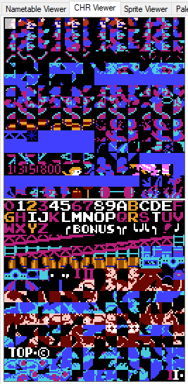
Now that we have manually mapped the CHR-ROM, we can try displaying our Pattern Tables. For simplicity’s sake, I will just use 4 different shades of white / grey / black, as we don’t have any palettes in the Pattern Tables.
Note: There is enough information available, to actually emulate a pixel pipeline through 2 x 16-bit and 2 x 8-bit shift registers, but I thought this could be a little bit of over-engineering for a NES emulator. So I went for the simpler approach at hand.
So, I created an SDL window, with a 128 x 256 texture, and now I fill every pixel with the appropriate 2-bit value (or rather, the assigned shade of grey for the 2-bit value).
for (int r = 0; r < 256; r++) {
	for (int col = 0; col < 128; col++) {
		uint16_t adr = (r / 8 * 0x100) + (r % 8) + (col / 8) * 0x10;
		uint8_t pixel = ((VRAM[adr] >> (7-(col % 8))) & 1) + ((VRAM[adr + 8] >> (7-(col % 8))) & 1) * 2;
		framebuffer_chr[(r * 128 * 3) + (col * 3)] = COLORS[pixel];
		framebuffer_chr[(r * 128 * 3) + (col * 3) + 1] = COLORS[pixel];
		framebuffer_chr[(r * 128 * 3) + (col * 3) + 2] = COLORS[pixel];
	}
}

SDL_UpdateTexture(texture_chr, NULL, framebuffer_chr, 128 * sizeof(unsigned char) * 3);
SDL_RenderCopy(renderer_chr, texture_chr, NULL, NULL);
SDL_RenderPresent(renderer_chr);
The only ‘magic’ happening here, is in line 4, where I get the according bit of the first byte, and add twice the according bit of the second byte for that pixel. Then we look up the value in our (grey-shaded) color palette, and assign the R, G and B values of our framebuffer array with these values.
So, after fiddling around a bit, until our magic line works out, we can eventually come up with this:
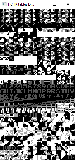
Looks about right! So, now that we have the Pattern Table at our hands, of course we want to display the actual VRAM.
ppu registers
Up to this point, our CPU might run flawlessly, but our VRAM is still empty. The VRAM is 16 kbytes of memory, that only the PPU has access to, so the CPU is not able to write to it. The only way, the CPU is able to move data to the PPU and the VRAM is through accessing the PPU registers, that the PPU offers.
| ADDRESS | NAME | WRITE | READ |
| 0x2000 | PPUCTRL | Sets multiple control bits for PPU | – |
| 0x2001 | PPUMASK | Controls draw order, switches | – |
| 0x2002 | PPUSTATUS | – | Shows VBLANK an Sprite info |
| 0x2003 | OAMADDR | Sets OAM starting address | – |
| 0x2004 | OAMDATA | Writes data to OAM | Reads the current OAM value |
| 0x2005 | PPUSCROLL | (2x) Controls screen scrolling | – |
| 0x2006 | PPUADDR | (2x) Sets address where PPUDATA shall write to | – |
| 0x2007 | PPUDATA | Writes to VRAM | – |
| 0x4014 | OAMDMA | Transfers 256 bytes to OAM from offset value | – |
PPUCTRL (0x2000)
7  bit  0
---- ----
VPHB SINN
|||| ||||
|||| ||++- Base nametable address
|||| ||    (0 = $2000; 1 = $2400; 2 = $2800; 3 = $2C00)
|||| |+--- VRAM address increment per CPU read/write of PPUDATA
|||| |     (0: add 1, going across; 1: add 32, going down)
|||| +---- Sprite pattern table address for 8x8 sprites
||||       (0: $0000; 1: $1000; ignored in 8x16 mode)
|||+------ Background pattern table address (0: $0000; 1: $1000)
||+------- Sprite size (0: 8x8 pixels; 1: 8x16 pixels)
|+-------- PPU master/slave select
|          (0: read backdrop from EXT pins; 1: output color on EXT pins)
+--------- Generate an NMI at the start of the
           vertical blanking interval (0: off; 1: on)
PPUMASK (0x2001)
7  bit  0
---- ----
BGRs bMmG
|||| |||| |||| |||+- Greyscale (0: normal color, 1: produce a greyscale display)
|||| ||+-- 1: Show background in leftmost 8 pixels of screen, 0: Hide
|||| |+--- 1: Show sprites in leftmost 8 pixels of screen, 0: Hide
|||| +---- 1: Show background
|||+------ 1: Show sprites
||+------- Emphasize red
|+-------- Emphasize green
+--------- Emphasize blue
PPUSTATUS (0x2002)
7  bit  0
---- ----
VSO. ....
|||| |||| |||+-++++- Least significant bits previously written into a PPU register
|||        (due to register not being updated for this address)
||+------- Sprite overflow. The intent was for this flag to be set
||         whenever more than eight sprites appear on a scanline, but a
||         hardware bug causes the actual behavior to be more complicated
||         and generate false positives as well as false negatives; see
||         PPU sprite evaluation. This flag is set during sprite
||         evaluation and cleared at dot 1 (the second dot) of the
||         pre-render line.
|+-------- Sprite 0 Hit.  Set when a nonzero pixel of sprite 0 overlaps
|          a nonzero background pixel; cleared at dot 1 of the pre-render
|          line.  Used for raster timing.
+--------- Vertical blank has started (0: not in vblank; 1: in vblank).
           Set at dot 1 of line 241 (the line *after* the post-render line);
           cleared after reading $2002 and at dot 1 of the pre-render line.
OAMADDR (0x2003) / OAMDATA (0x2004)
Writing to OAMDATA writes to the OAM at the address OAMADDR. OAM is a separate memory connected to the PPU, it is not inside the VRAM!
PPUSCROLL (0x2005)
Write twice, to store the offset of the viewport to the VRAM, so we can scroll the viewport around the VRAM. First byte written is X-offset, second byte is Y-offset.
PPUADDR (0x2006)
Write twice, to store the address that PPUDATA will write to. First byte sent is the high byte, second is the low byte.
PPUDATA (0x2007)
Write to this register, to actually store data in VRAM, at address PPUADDR (increased after write).
OAMDMA(0x4014)
When written to this register, a OAM DMA transfer of 256 bytes will be started, reading from memory[val << 8] to OAM[OAMADDR]. So the value sent to OAMDMA is the actual page the CPU will fetch the 256 bytes from.
So, for all these registers we will need to implement the interfaces for it, so we can have a proper interface to our PPU. I implemented this in my MMU, so I can prevent the actual memory writes, and redirect them to the appropriate PPU functions, for the PPU to handle them. This way, we can ensure that “Donkey Kong” can populate the VRAM properly.
void writeToMem(uint16_t adr, uint8_t val) {

	switch (adr) {
		case 0x2000:		//	PPUCTRL
			writePPUCTRL(val);
			break;
		case 0x2003:		//	OAMADDR
			writeOAMADDR(val);
			break;
		case 0x2004:		//	OAMDATA
			writeOAMDATA(val);
			break;
...
Comments