The C64 has something called PLA (Programmable Logic Array), which can be accessed through the Zeropage at 0x0001. This little thing is capable of banking the memory, and switching components that are accesible at certain memory ranges.
This is, why we don’t actually work with a 6502 like the NES, but rather with a 6510!
For now, the only thing we are interested in, are the lower 3 bits, because they are solely responsible for the banking.
0x0001 (PLA)
bit 0 - LORAM
bit 1 - HIRAM
bit 2 - CHAREN
With the combinations possible of these 3 bits, we are able to represent multiple layouts of banking:
        Bit+-------------+-----------+------------+
        210| $8000-$BFFF |$D000-$DFFF|$E000-$FFFF |
   +---+---+-------------+-----------+------------+
   | 7 |111| Cart.+Basic |    I/O    | Kernal ROM |
   +---+---+-------------+-----------+------------+
   | 6 |110|     RAM     |    I/O    | Kernal ROM |
   +---+---+-------------+-----------+------------+
   | 5 |101|     RAM     |    I/O    |    RAM     |
   +---+---+-------------+-----------+------------+
   | 4 |100|     RAM     |    RAM    |    RAM     |
   +---+---+-------------+-----------+------------+
   | 3 |011| Cart.+Basic | Char. ROM | Kernal ROM |
   +---+---+-------------+-----------+------------+
   | 2 |010|     RAM     | Char. ROM | Kernal ROM |
   +---+---+-------------+-----------+------------+
   | 1 |001|     RAM     | Char. ROM |    RAM     |
   +---+---+-------------+-----------+------------+
   | 0 |000|     RAM     |    RAM    |    RAM     |
   +---+---+-------------+-----------+------------+
        |||
  /CharEn|/LoRam
         |
       /HiRam

(credits unusedino.de)
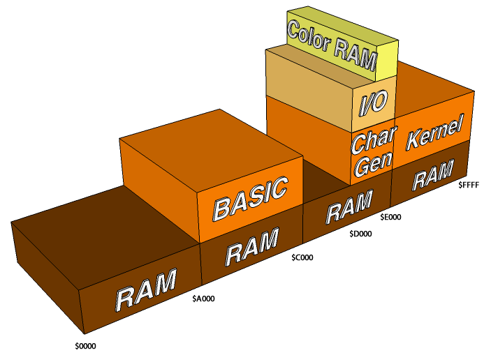
So this shows, and dictactes, which components are visible to the CPU! Therefore it is crucial, that we implement this in our address management where we handle reads and writes, because games / programs might just disable the Kernal and I/O, to store more data there.
if (!LORAM && !HIRAM) {
		memtype_a000_bfff = MEMTYPE::RAM;
		memtype_d000_dfff = MEMTYPE::RAM;
		memtype_e000_ffff = MEMTYPE::RAM;
	}
	else if (LORAM && !HIRAM) {
		memtype_a000_bfff = MEMTYPE::RAM;
		memtype_e000_ffff = MEMTYPE::RAM;
	}
	else if (!LORAM && HIRAM) {
		memtype_a000_bfff = MEMTYPE::RAM;
		memtype_e000_ffff = MEMTYPE::KERNAL;
	}
	else if (LORAM && HIRAM) {
		memtype_a000_bfff = MEMTYPE::BASIC;
		memtype_e000_ffff = MEMTYPE::KERNAL;
	}
	if (!CHAREN) {
		if (LORAM || HIRAM) {
			memtype_d000_dfff = MEMTYPE::CHARROM;
		}
	}
	else if (CHAREN) {
		if (LORAM || HIRAM) {
			memtype_d000_dfff = MEMTYPE::IO;
		}
	}
As you can see, there is quite a lot we can address with this schema.
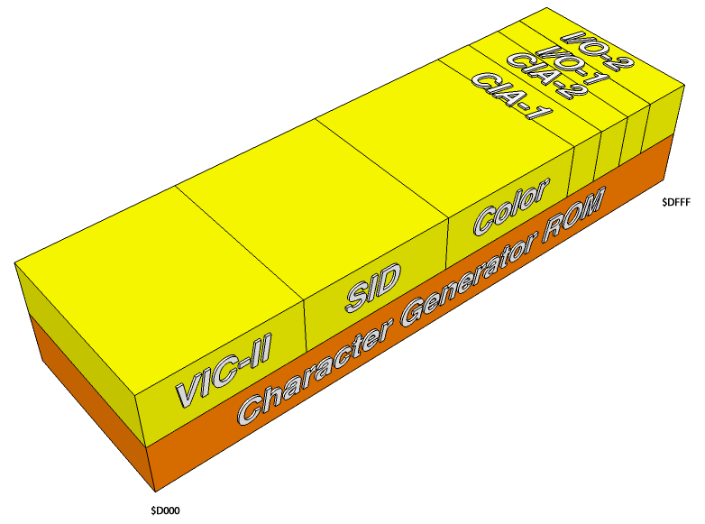
Note: The ColorRAM is part of the I/O and therefore enabled/disabled (for the CPUs eyes) with it by the PLA.
How does the VIC handle this?
Another thing worth noting is, the VIC/PPU is always looking at RAM. With two little exceptions:
- ColorRAM is always accessible (the VIC has 4 lines directly wired to ColorRAM)
- When the VIC is mapped to bank 0 or bank 2, at the (relative to the 16K window) address 0x1000 – 0x1fff is the CHRROM (CharGen)
With the PLA logic implemented, it’s our next step to get our first PRGs to load, so we can implement and test things like graphics modes, and more! So, this will be our next chapter.