As mentioned earlier, the SNES can address 16megs of address space. Some of it is WRAM, some is SRAM, some is cartridge ROM, some are address- and data-registers (MMIO) for external components such as CGRAM, VRAM etc.
To visualize and describe the memory map and its components a bit better, we start off by dividing the space into 4 quadrants.
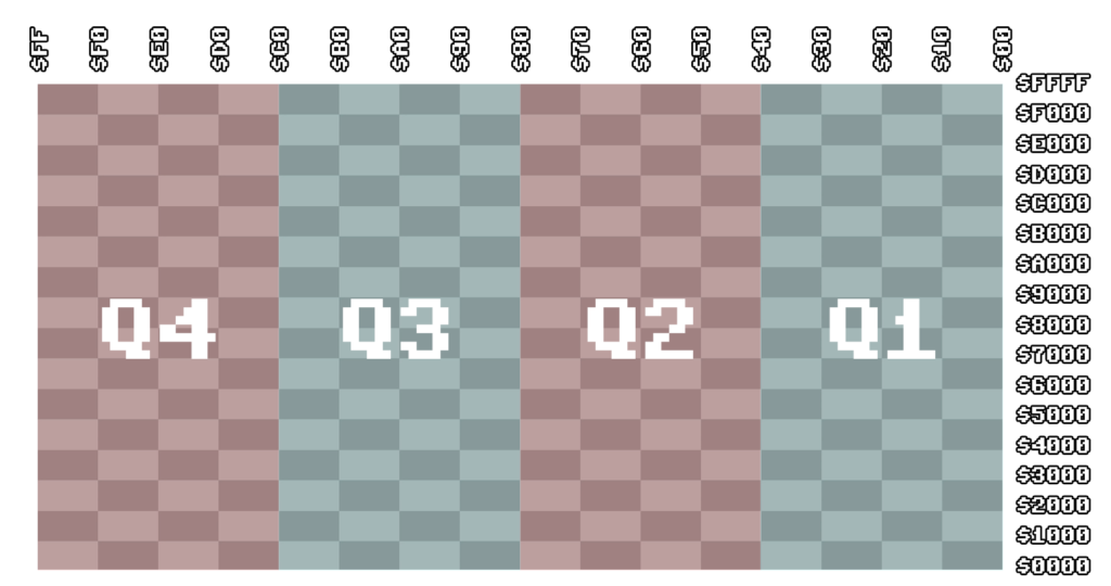
On top you can see the different banks, on the right side you can see the 64k of space addressable on each bank.
Now, not the full 16megs are available to the games, but certain areas already have been defined and mapped.
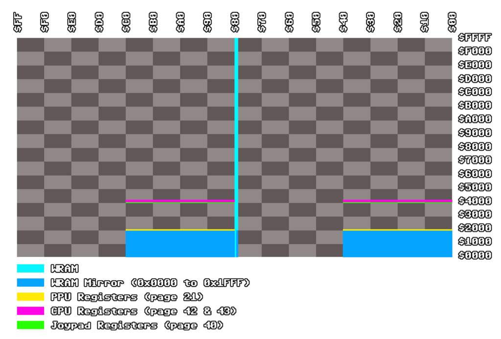
WRAM is living in a fixed space of banks 0x7E and 0x7F. The first 32 pages of WRAM (0x7E0000 to 0x7E1FFF) are mirrored across quadrants 1 and 3.
Meaning, accessing e.g. 0xBB1234 accesses the same memory as 0x7E1234 or 0x111234.
PPU registers are available at various addresses in page 21. This is (next to DMAs) the only option to interact with the PPU and VRAM.
CPU registers are available at various addresses in page 42 and 43.
Joypad registers are available in a few bytes in page 40.
The rest of the memory map is theoretically freely availble for anything else, even though there are (of course) some quirks and conventions that were followed. For now the most important convention to us is ROMSEL, the are where we are allowed to map our games to.
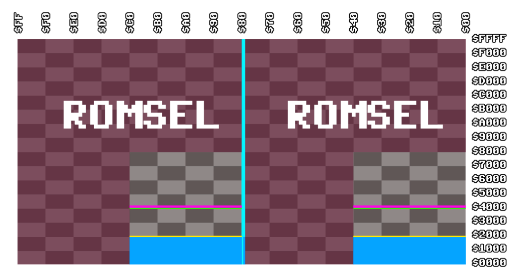
ROMSEL areas are, as you can see, all upper halfs of our quadrants, and the lower halfs of Q2 and Q4. If a ROM is small, it will get mirrored all over the ROMSEL space (I will go into more detail of how and where later on).
Just keep in mind that the upper half of Q2 is not fully available, since 2 banks are already occupied by WRAM.
mappers
How those areas are filled, is dependant on the mapper mode though. The most common ones are the following:
| Mode 0 / 20 | LoROM |
| Mode 1 / 21 | HiROM |
| Mode 2 / 22 / 2a | Super MMC |
| Mode 3 / 23 | SAS |
| Mode 4 / 24 | SFX |
| Mode 5 / 25 | ExHiROM |
LoROM
This is the simplest mapper of them all. Nevertheless it is important to notice that the information about mappers here is a general rule of thumb, in the end there can be numerous variations of said mappers, depending on the wiring on the cartridge.
The LoROM mapper works by mapping the first half bank of the ROM to the upper half of Q3, more specifically bank $80 (so, from 0x808000 to 0x80FFFF). The next half bank is then mapped to the upper half of bank $81. This pattern continues, until the ROM is completely mapped (to the upper half of Q3 – and Q4 if it is large enough).
The maximum ROM size in this mode is therefore 4 MB.
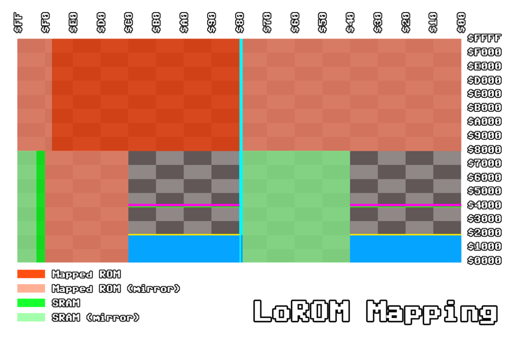
If the cartridge comes with SRAM, the SRAM will be mapped to the lower half of bank $F0, more specifically from 0xF00000 up to 0xF07FFF, so 32 kilobyte. If there is more than 32k of SRAM available, it will be mapped to the lower banks of the following banks up to bank $FF.
As you can already see in the image, the SRAM and the ROM get mirrored to the rest of the ROMSEL area that is available after mapping out the entire ROM. SRAM gets mirrored right after the actual SRAM mapping, on the lower half of the banks up to bank $FF. The same happens with the ROM, after it’s completely mapped, the mirroring starts in the upper halfs of the banks of Q3/4 (depending on the ROMs size), up to bank $FF.
The entire state of Q3 and Q4 now is mirrored to the ROMSEL area in Q1 and Q2. Because of the WRAM area in Q2, if the ROM / SRAM are big enough, there may be parts that can only be accessed through Q4!
With this information we are now able to create a rudimentary memory mapping, because the test ROMs for now will only be LoROM. So we can make sure we have the basics implemented. Other mappers, such as HiROM will be implemented later in the process.
//	copy cartridge to memory
void loadROM(string filename) {

	//	load cartridge to memory
	cartridge_memory = readFile(filename.c_str());

	//	identify cartridge & post data to variable
	u16 base_snes_header = 0xffff;
	bool isLoROM = true;
	u16 filesizeInKb = cartridge_memory.size() / 1024;
	if (isLoROM) {
		base_snes_header = 0x8000;

		//	map rom to memory
		u8 bank = 0x80;
		u8 shadow_bank = 0x00;
		u8 chunks = filesizeInKb / 32;		//	LoRAM stores 32kb chunks, so we want to know how many chunks it takes up before the first mirroring (has to) appear
		for (u32 i = 0; i < cartridge_memory.size(); i++) {

			//	write to all locations that mirror our ROM
			for (u8 mirror = 0; mirror < (0x80 / chunks); mirror++) {

				//	(Q3-Q4) 32k (0x8000) consecutive chunks to banks 0x80-0xff, upper halfs (0x8000-0xffff)
				if ((bank + (i / 0x8000) + (mirror * chunks)) < 0xff) {
					memory[((bank + (i / 0x8000) + (mirror * chunks)) << 16) | 0x8000 + (i % 0x8000)] = cartridge_memory[i];
				}

				//	(Q1-Q2) shadowing to banks 0x00-0x7d, except WRAM (bank 0x7e/0x7f)
				if ((shadow_bank + (i / 0x8000) + (mirror * chunks)) < 0x7e) {
					memory[((shadow_bank + (i / 0x8000) + (mirror * chunks)) << 16) | 0x8000 + (i % 0x8000)] = cartridge_memory[i];
				}

			}

		}

	}
...
}
Really nice diagrams of memory layout!
Thanks, glad you like it 🙂