
The only way to communicate with the PPU, and therefore VRAM and CGRAM, is through some fixed registers that we already talked about in the memory mapping section. VRAM stores things like tilemaps and tiles, while CGRAM stores colors and palettes.
CGRAM
CGRAM is 256 16-bit words large (so 512bytes in total). Depening on the mode the PPU is running on currently, the colors / palettes are stored a little bit differently.
Each color is represented by 2 bytes (16 bits), of those only 15 bits are actually used. The lowest 5 bits for red, the following 5 bits for green and the next following 5 bits for blue. The last bit (MSB) isn’t used at all and should always be zero.
This format can easily be rendered with SDL2 with its Pixelformat BGR555
The color with index 0 on each color palette is always transparent, and will show any underlying pixels (or, the backdrop color if there are none).
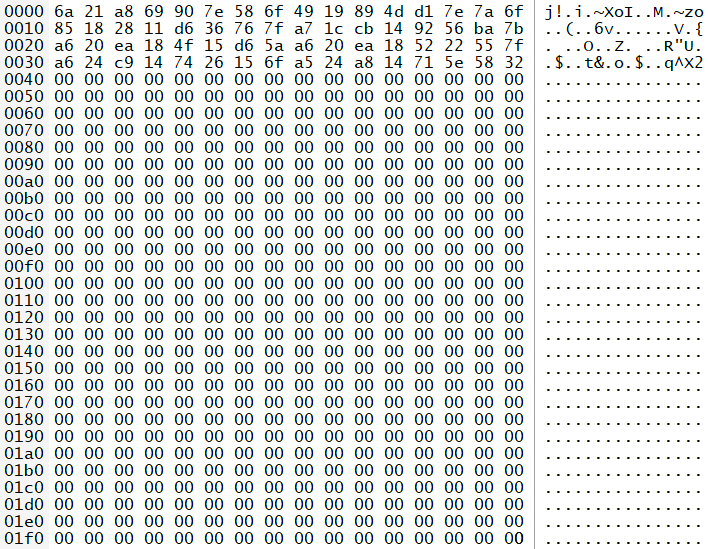
To communicate with the CGRAM, we have a 2 registers for this, the CGRAM Address register at 0x2121, and the CGRAM Data register at 0x2122.
The CGRAM Address register simply indicates the destination in the CGRAM that we want to write to (0x00 – 0xFF). Writing to the CGRAM Data register stores the actual value. But, since CGRAM holds 16-bit words, we need to write to it twice.
Internally this is handled by a flipflop, that will cache the first write (LSB) and OR it with the second write (MSB) to write it to CGRAM.
This is how colors are stored in CGRAM.
VRAM
VRAM works in a similar way to CGRAM, and consists of 32k 16-bit words (so 64kb in total). Again we have Data and Address registers. Thankfully for the VRAM we don’t have to emulate a flipflop, but we have 2 addresses to write the low- and high-bytes of the target address separately.
0x2116 VRAM Address lower byte (W)
0x2117 VRAM Address upper byte (W)
By writing to these 2 Addresses we have set the target address to where in the VRAM we want to write. Now we have the 2 Data Write registers, which allow us to write the both bytes to said location.
0x2118 VRAM Data Write lower byte (W)
0x2119 VRAM Data Write upper byte (W)
This is the only method to transfer data to VRAM.
There are 2 additional registers, only for reading values from VRAM, from the address set at 0x2116 / 0x2117.
0x2139 VRAM Read lower byte (R)
0x213A VRAM Read upper byte (R)
Tiles
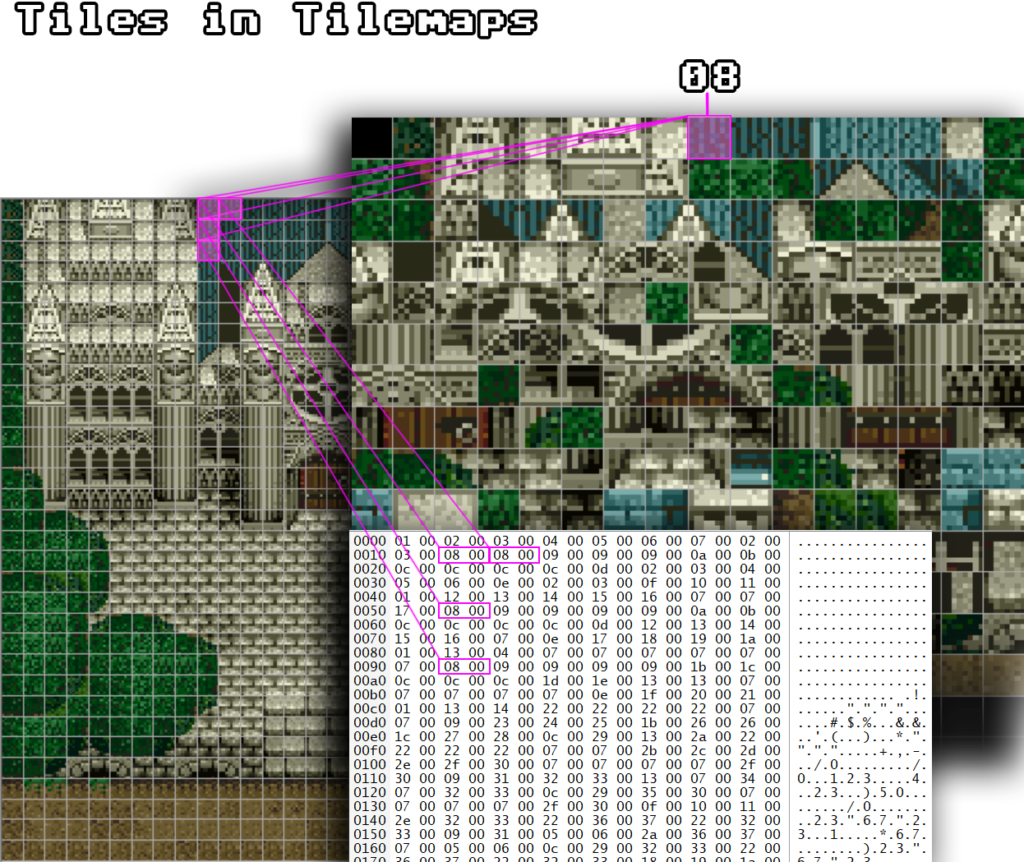
VRAM gets filled with stuff like Tilemaps and Tiles for example. Tiles are usually 8×8 pixels (other formats are possible, but will be ignored for this chaper for complexity’s sake) big, pieces that can be stored anywhere in VRAM. The Tiles are the catalogue of graphical pieces, we can put on our Background with the Tilemap.
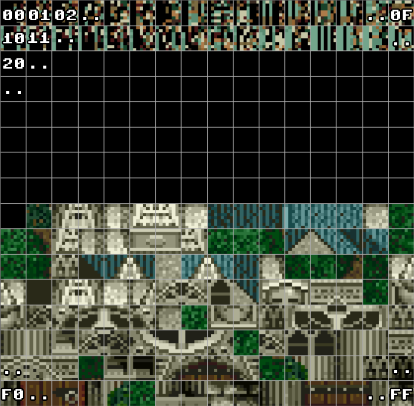
Tiles have indices through which they can be selected. So, Tilemaps only have to store the index of the tile, and the actual data can then be fetched from the Tiles themselves.
For the PPU to find and load Tiles properly, we have registers that will indicate the beginning of the memory regions where Tiles are being stored.
0x210B / 0x210C
Bits 00-03 – BG1 Tile Base Address
Bits 04-07 – BG2 Tile Base Address
Bits 08-11 – BG3 Tile Base Address
Bits 12-15 – BG4 Tile Base Address
The value of these registers is then multiplied by 0x2000, and then modulo’d with 0x10000, which is the base address (byte-aligned) of the tiles for the individual Background (BG).
Tilemaps
The same logic applies for the Tilemaps themselves, we can set the start address for the tilemaps with the following registers.
0x2107 – BG1 Base Address and Screen Size
0x2108 – BG2 Base Address and Screen Size
0x2109 – BG3 Base Address and Screen Size
0x210A – BG4 Base Address and Screen Size
Bits 0-1 / Screen Size
00 – 32×32 Tiles
01 – 64×32 Tiles
10 – 32×64 Tiles
11 – 64×64 Tiles
Bits 2-7 / BG Base Address
Shift this value 10bits to the left to have the actual BG Base Address
Example:
Value 0xFC is stored at 0x2107 (BG1). Binary representation is 1111 1100. Bits 0 and 1 show a 00, indicating that we have 32×32 tiles. Bits 2-7 show 1 1111. Shifting these bits to the left 10 times (16-bit limits) we will come up with 0xFC00, which then will be the starting address of the tilemap for Background 1.
Tilemaps themselves, as you can see in the last images memory representation, holds the indices of the tiles that are supposed to be put into place. Each entry in VRAM is of course a 16-bit value.
Bits 0-9 will form the Tile ID, bits 10-12 will define the Palette id of this Tile.
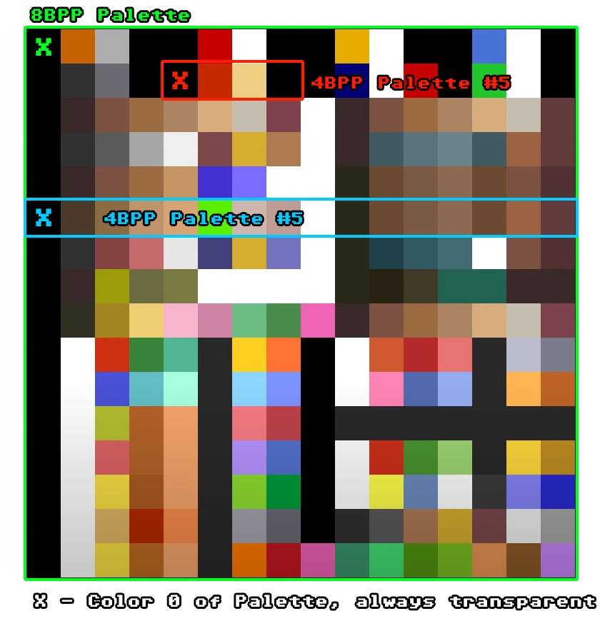
Palettes
One of the most powerful tools for a SNES dev was to use palettes for his tiles. This would give you the option to create multiple versions of a single graphic, for example in Super Mario World you have red and green shells, or pipes that have different colors etc.
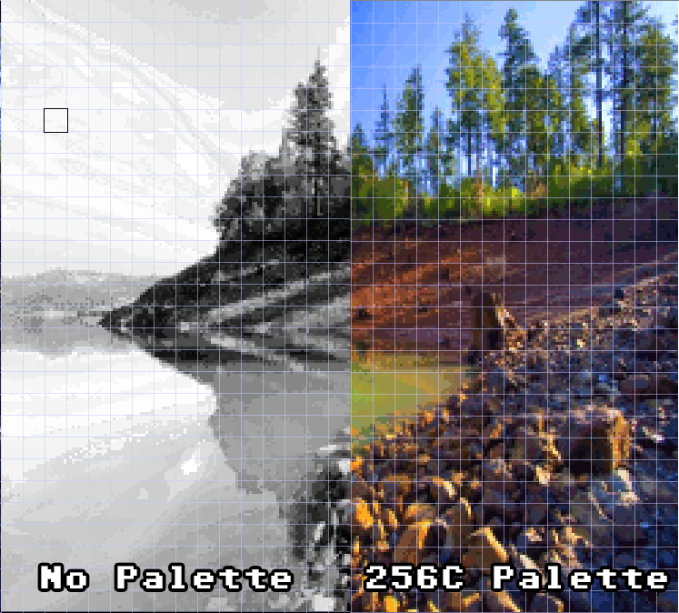
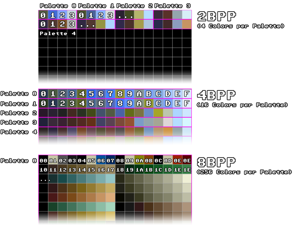
As already mentioned, colors and therefore palettes are stored in CGRAM. The amount of colors available for a palette depends on the mode the current BG is running in. For now we will look at 4-Color-Mode (2BPP), 16-Color-Mode (4BPP) and 256-Color-Mode (8BPP). We will get into more detail of Backgrounds and Modes in the next chapter.
For now we only need to know how the palettes work in regards of Color Depth. 2BPP for example gives us 2 Bits Per Pixel. 2 Bits give us 4 total states, thus 4 available colors. 8BPP gives us 8 Bits Per Pixel, therefore 256 possible states, therefore 256 available colors. The same logic goes for 4BPP.
You will now notice, that the higher the BPP mode, the more bytes a Tile will take up to be formed, and the more space the Palette(s) take up in CGRAM.
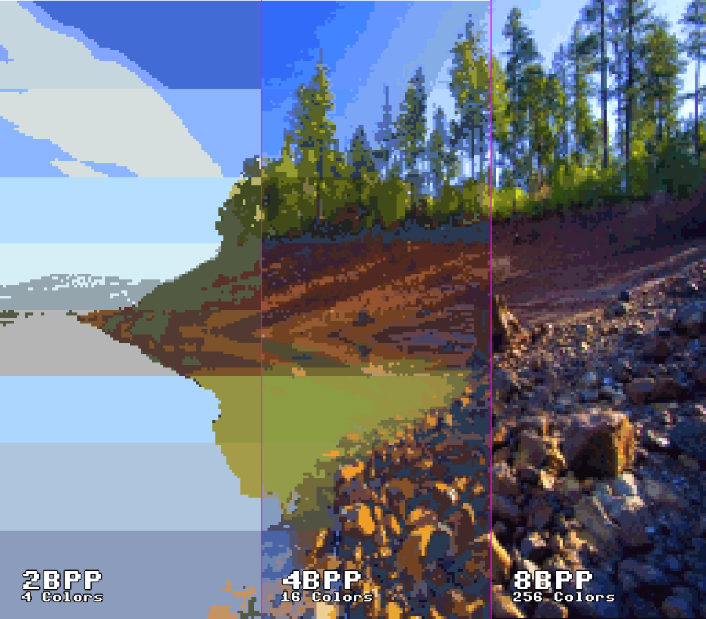
When 8BPP mode occupies the complete CGRAM to store all of its 256 colors, 4BPP and 2BPP modes have multiple palettes across CGRAM, so the tiles can select one of those palettes for them to use.
All these information can now be coded into our Bus like this:
void writeToMem(u8 val, u32 fulladr) {
	u8 bank_nr = fulladr >> 16;
	u16 adr = fulladr & 0xffff;
 	switch (bank_nr) {
	case 0x00:
		switch (adr)
		{
...
			//	PPU	Data Write
		case 0x2118:
			PPU_writeVRAMhigh(val, (memory[0x2117] << 8) | memory[0x2116]);
			break;
		case 0x2119:
			PPU_writeVRAMlow(val, (memory[0x2117] << 8) | memory[0x2116]);
			break;
...
			//	PPU - CGDATA - Palette CGRAM Data Write (W)
		case 0x2122:
			PPU_writeCGRAM(val, memory[0x2121]);
			break;
And accordingly in our PPU:
...
u16 VRAM[0x8000];	//	64 kbytes (16bit * 0x8000 [ 32768 ] )
u16 CGRAM[0x100];	//	512 bytes (16bit * 0x100 [ 256 ] )

void PPU_writeVRAMlow(u8 val, u16 adr) {
	VRAM[adr & 0x7fff] = (VRAM[adr & 0x7fff] & 0xff00) | val;
}

void PPU_writeVRAMhigh(u8 val, u16 adr) {
	VRAM[adr & 0x7fff] = (VRAM[adr & 0x7fff] & 0xff) | (val << 8);
}

u16 PPU_readVRAM(u16 adr) {
	return VRAM[adr & 0x7fff];
}

void PPU_writeCGRAM(u8 val, u8 adr) {
	//	if address is even, we just remember the current value
	if (!CGRAM_Flipflop) {
		CGRAM_Lsb = val;
		CGRAM_Flipflop = true;
	}
	//	else concat the remembered value with the current one, and store it to adr-1
	else {
		CGRAM[adr] = (val << 8) | CGRAM_Lsb;
		CGRAM_Flipflop = false;
		writeToMem(readFromMem(0x2121) + 1, 0x2121);
	}
}

u16 PPU_readCGRAM(u8 adr) {
	return CGRAM[adr];
}
...
VRAM address auto-increase and address translation
There is the additional register 0x2115 which offers to automatically manipulate the VRAM Address on access. This is of great use for example for DMAs, and Bitmap graphics etc.
The actual bits of this register correspond to the following:
| 7 | Increment VRAM Address after accessing High/Low byte (0=Low, 1=High) |
| 6-4 | Unused |
| 3-2 | Address Translation (0..3 = none, 8bit, 9bit, 10bit) |
| 1-0 | Address Increment Step (0..3 = increment word-address by 1,32,128,128) |
The actual address translation (when needed) is handled like this:
   Translation  Bitmap Type              Port [2116h/17h]    VRAM Word-Address   8bit rotate  4-color;   1 word/plane    aaaaaaaaYYYxxxxx --> aaaaaaaaxxxxxYYY   9bit rotate  16-color;  2 words/plane   aaaaaaaYYYxxxxxP --> aaaaaaaxxxxxPYYY   10bit rotate 256-color; 4 words/plane   aaaaaaYYYxxxxxPP --> aaaaaaxxxxxPPYYY

"aaaaa" - normal address MSBs
"YYY"   - Y-index (within a 8x8 tile)
"xxxxx" - selects one of the 32 tiles per line
"PP"    - bit-plane index (for BGs with more than one Word per plane).

(thanks no$)
The technical translation is a triple-left-shift of the lower 8, 9 or 10 bits, to get the Y-index to the 3 LSBs.
We add this automatic address increase and the address translation functionalities to our recent code:
...
u8 _v_hi_lo = memory[0x2115] >> 7;
u8 _v_trans = (memory[0x2115] & 0b1100) >> 2;
u8 _v_step = memory[0x2115] & 0b11;
switch (_v_trans) {		//	PPU - Apply address translation if necessary (leftshift thrice lower 8, 9 or 10 bits)
	case 0b00:
		break;
	case 0b01: {		//	8 bit, aaaaaaaYYYxxxxx becomes aaaaaaaxxxxxYYY
		u16 _t_st = (_adr & 0b1111111100000000);
		u16 _t_off = (_adr & 0b11100000) >> 5;
		u16 _t_in = (_adr & 0b11111) << 3;
		_adr = _t_st | _t_off | _t_in;
		break;
	}
	case 0b10: {		//	9 bit, aaaaaaYYYxxxxxP becomes aaaaaaxxxxxPYYY
		u16 _t_st = (_adr & 0b1111111000000000);
		u16 _t_off = (_adr & 0b111000000) >> 6;
		u16 _t_in = (_adr & 0b111111) << 3;
		_adr = _t_st | _t_off | _t_in;
		break;
	}
	case 0b11: {		//	10 bit, aaaaaYYYxxxxxPP becomes aaaaaxxxxxPPYYY
		u16 _t_st = (_adr & 0b1111110000000000);
		u16 _t_off = (_adr & 0b1110000000) >> 7;
		u16 _t_in = (_adr & 0b1111111) << 3;
		_adr = _t_st | _t_off | _t_in;
		break;
	}
}
if ((adr == 0x2118 && !_v_hi_lo) || (adr == 0x2119 && _v_hi_lo)) {
	u16 _t = _adr;
	switch (_v_step)
	{
		case 0b00: _t += 1;	break;
		case 0b01: _t += 32; break;
		case 0b10: _t += 128; break;
		case 0b11: _t += 128; break;
		default: break;
	}
	memory[0x2116] = _t & 0xff;
	memory[0x2117] = _t >> 8;
}
VBlank NMIs
Another important step to get graphical tests running, is to handle the RDNMI Register, which indicates to the software that the VBlank period was reached. VBlank defines the are where the raster beam of the TV reached the end of the screen, is turned off and brought back to the beginning of the screen. So in this period of time there is no drawing, that’s why software will often do crucial VRAM updates in this periods to avoid glitching, which could occure when you change VRAM components while the screen is being drawn.
The RDMNI Register is located at 0x4210. The only important bit is bit 7.
0 = None
1 = Interrupt Request (Begin of VBlank)
The lower bits will always return 2, the version code of the CPU. So make sure to return 0x82 (Interrupt Request) or 0x02 (None).
Whenever the register is being read from software, and bit 7 is set, it will immediately be reset (acknowledged).
For now you can just change the value whenever it’s being read (it’s enough to run the tests), but we will have to implement proper timing for this later on (how many master- and dot-cycles it will take for a single row to be rendered, and when VBlank is exactly reached).
In the next chapter we will cover some modes, and the multiple available Backgrounds and the blending of them, which we will be able to test and show with more of krom’s awesome tests.
Comments